
Electronics & PCB Re-engineering
Revolutionize electronics reconstruction using computer vision pipelines, X-ray tomography, and automated via/trace detection for comprehensive PCB analysis and reverse engineering.
Proven foundations for modern web products
AI-Powered Electronics Reconstruction
Our electronics and PCB re-engineering service combines cutting-edge computer vision, X-ray tomography, and deep learning to provide non-destructive analysis and complete reconstruction of electronic systems. From component identification to trace connectivity mapping, we deliver unprecedented accuracy and efficiency.
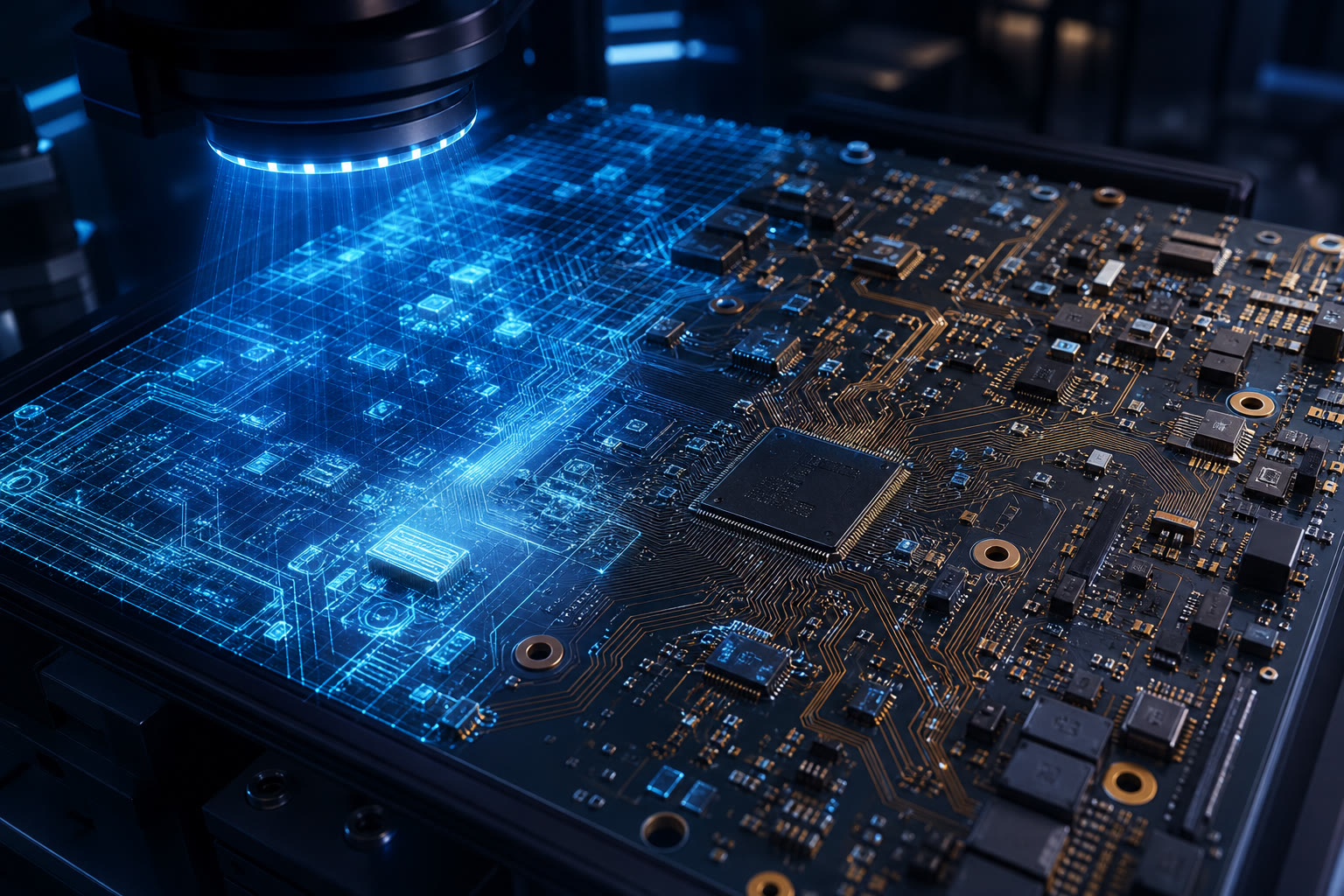
Computer Vision & AI Capabilities
Advanced computer vision and AI-powered tools specifically designed for electronics analysis, PCB reconstruction, and non-destructive testing applications.
Computer Vision Pipelines
Advanced computer vision pipelines specifically designed for PCB reverse engineering and component identification.
Key Features
- Multi-spectral image analysis
- Component recognition algorithms
- Layer separation techniques
- Pattern matching systems
- 3D reconstruction capabilities
Benefits
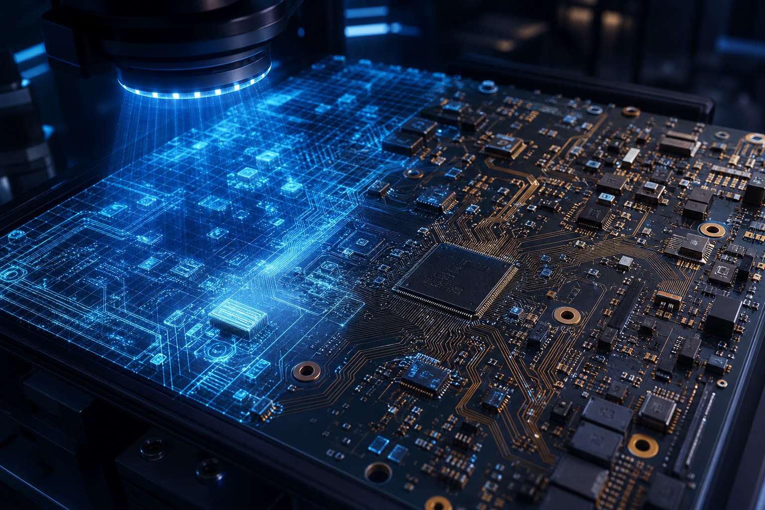
Non-destructive Reconstruction
X-ray tomography based non-destructive analysis for complete PCB reconstruction without component removal.
Key Features
- High-resolution X-ray imaging
- 3D volumetric reconstruction
- Internal structure analysis
- Multi-layer board examination
- Component interaction mapping
Benefits
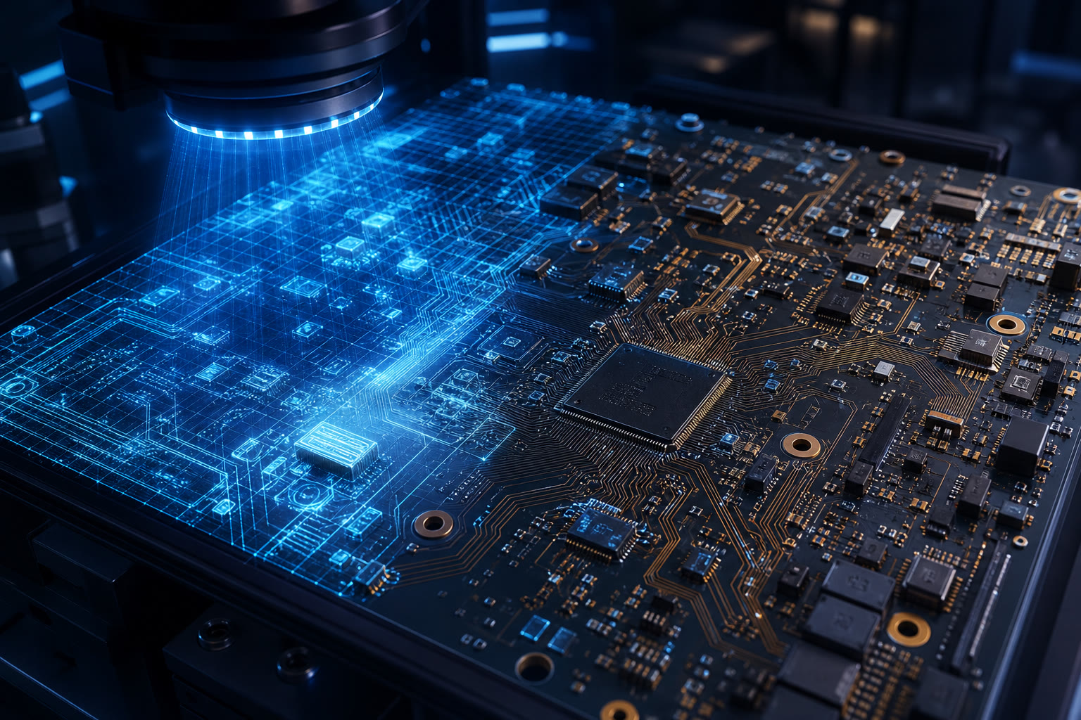
Automated Via/Trace Detection
Intelligent automated detection and connectivity extraction for vias, traces, and electrical connections.
Key Features
- AI-powered trace following
- Via detection algorithms
- Connectivity mapping
- Layer transition tracking
- Electrical property inference
Benefits
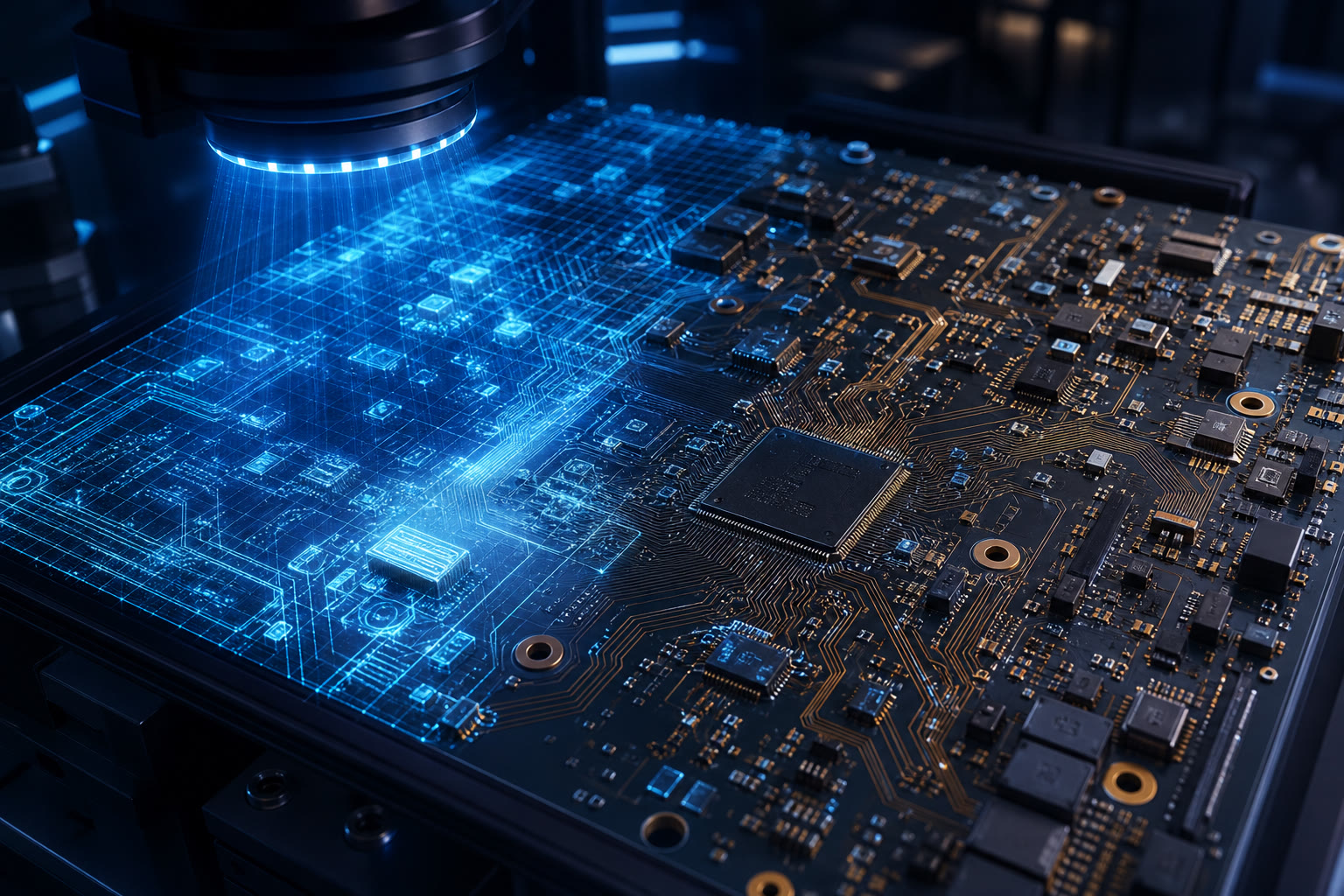
Deep Learning Defect Detection
Advanced deep learning models for automated optical inspection (AOI) and defect detection in electronics manufacturing.
Key Features
- Multi-class defect classification
- Real-time AOI processing
- Anomaly detection algorithms
- Quality assurance automation
- Predictive defect analysis
Benefits
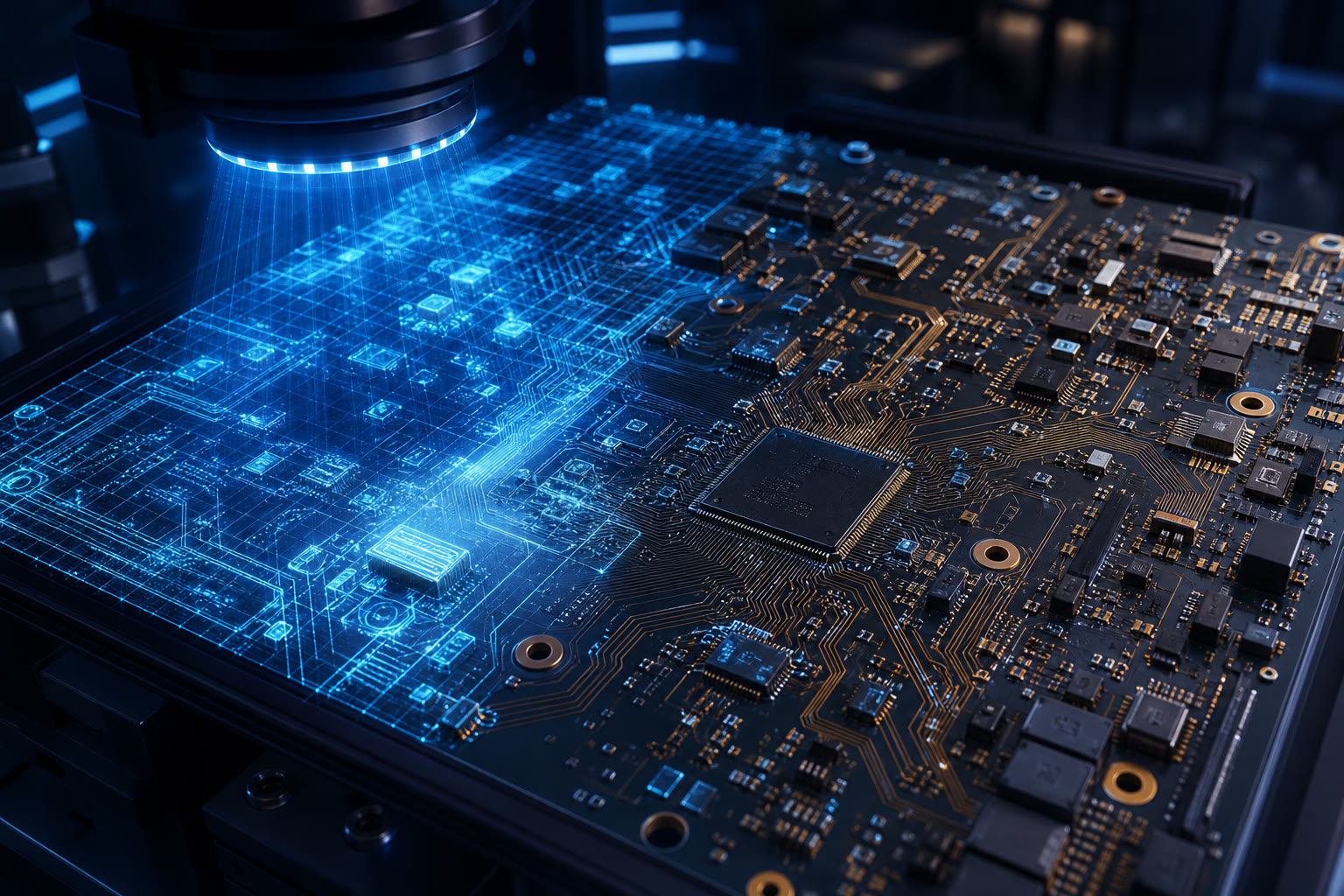
Electronics Analysis Process
A comprehensive approach to electronics and PCB analysis that combines computer vision, X-ray imaging, and deep learning for complete system reconstruction.
1. Visual Analysis
Advanced computer vision pipelines for component identification and pattern recognition.
2. X-ray Imaging
High-resolution X-ray tomography for non-destructive internal structure analysis.
3. Trace Mapping
Automated via and trace detection with complete connectivity extraction.
4. Defect Detection
Deep learning AOI for comprehensive defect detection and quality assurance.
Ready to Transform Your Business with AI?
Join hundreds of companies that have already revolutionized their operations with our AI-driven re-engineering solutions.
Trusted by leading companies worldwide
Email Us
nikflipflop@gmail.com
Call Us
+380-50-97-38-170
Visit Us
Bannyi Lane, 1
Kharkiv, 61000, Ukraine