
Consumer Technology
Non-destructive reconstruction of proprietary industrial control PCB designs for legacy system modernization and supply chain diversification
IndustrialControl Systems operates 340 manufacturing facilities worldwide with proprietary control PCB designs dating back 15+ years. These mission-critical boards control everything from assembly lines to chemical processes. Original schematics and manufacturing files were lost during corporate acquisitions and supplier changes. Each PCB contains 12-28 layers, 2,000-8,000 components, and controls processes worth $2.3B in annual revenue. Plant downtime due to PCB failures cost $47,000 per hour.
The lack of design documentation created dependency on single-source suppliers, vulnerability to supply chain disruptions, inability to implement improvements, and escalating maintenance costs averaging $12.3M annually across all facilities.
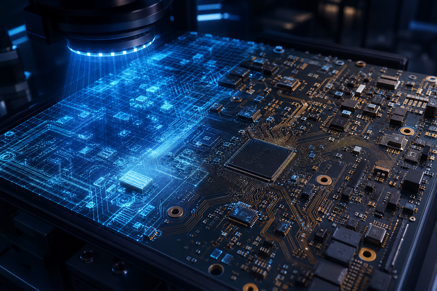
Computer vision pipelines for component detection, X-ray tomography for non-destructive analysis, automated via/trace detection and connectivity extraction, deep learning defect detection (AOI)
Deploy advanced imaging techniques including high-resolution photography, X-ray tomography, and 3D scanning. Use computer vision and machine learning for automated component identification, trace routing analysis, and connectivity mapping. Implement AI-powered defect detection for quality assurance.
from 73.2% (manual)
from 45.8%
from 67.3% (photogrammetry)
from 71.6%
from 0.8 boards/day
72% reduction
multiple supplier enablement
from 8.2 weeks
34% cost savings
from 24 weeks
"The AI-powered PCB reconstruction technology gave us complete control over our manufacturing destiny. The precision of the computer vision analysis and the completeness of the digital reconstruction exceeded our most optimistic expectations."
Get comprehensive technical analysis, implementation details, and performance metrics from this project.
technical report
technical report
Let us help you modernize your critical systems using our proven AI-driven re-engineering methodologies.
Chief Data Protection Officer
Languages: English, Ukrainian
Response Time: 24-48 hours for initial response